General DescriptionFSMOS® MOSFET is based on Oriental Semiconductor's unique device design to achieve low
RDS(ON) , low gate charge,
fast switching and excellent avalanche characteristics.
The high Vth series
is specially designed to use in motor control systems with driving voltage of more than 10V .Features Low RDS(ON)
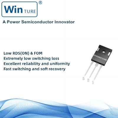
& FOM Extremely low switching loss Excellent reliability and uniformity Fast switching and soft recoveryApplications PD charger Motor driver Switching voltage regulator DC-DC convertor Switching mode power supplyKey Performance ParametersParameterValueUnitVDS80VID, pulse800ARDS(ON),
max @
VGS =10V1.9mΩQg144nCAbsolute Maximum Ratings at Tj =25°C unless otherwise notedParameterSymbolValueUnitDrain-source voltageVDS80VGate-source voltageVGS±20VContinuous drain current1)
, TC=25 °CID350APulsed drain current2) , TC=25
°CID, pulse800AContinuous diode forward current1)
, TC=25 °CIS350ADiode pulsed current2) , TC=25 °CIS,
pulse800APower dissipation3), TC=25
°CPD450WSingle pulsed avalanche energy4)EAS735mJOperation and storage temperatureTstg ,
Tj-55
to 175°CThermal CharacteristicsParameterSymbolValueUnitThermal resistance,
junction-caseRθJC0.33°C/WThermal resistance,
junction-ambientRθJA62°C/WElectrical Characteristics at Tj =25°C unless otherwise specifiedParameterSymbolMin.Typ.Max.UnitTest conditionDrain-source
breakdown voltageBVDSS80 VVGS =0
V, ID =250
μAGate thresholdvoltageVGS(th)2 4VVDS =VGS , ID =250
μADrain-sourceon-state resistanceRDS(ON) 1.51.9mΩVGS =10
V, ID=30
AGate-sourceleakage currentIGSS 100nAVGS =20
V - 100VGS =-20
VDrain-sourceleakage currentIDSS 1μAVDS =80 V,
VGS =0 VGate resistanceRG 1.2 Ωƒ=1 MHz,
Open drainDynamic CharacteristicsParameterSymbolMin.Typ.Max.UnitTest conditionInput capacitanceCiss 11200 pFVGS =0 V,VDS =25
V,ƒ=100
kHzOutput capacitanceCoss 4880 pFReverse transfer capacitanceCrss 221 pFTurn-on delay timetd(on) 31 nsVGS =10
V,VDS =50 V,RG=2
Ω,ID=25 ARise timetr 26 nsTurn-off delay timetd(off) 75 nsFall timetf 28 nsGate Charge CharacteristicsParameterSymbolMin.Typ.Max.UnitTest conditionTotal gate chargeQg 144 nCVGS =10
V,VDS =50
V,ID=25 AGate-source chargeQgs 40 nCGate-drain chargeQgd 22 nCGate plateau voltageVplateau 3.8 VBody Diode CharacteristicsParameterSymbolMin.Typ.Max.UnitTest conditionDiode forward voltageVSD 1.3VIS=30
A,VGS =0
VReverse recovery timetrr 123 nsVR=50 V,IS=25
A,di/dt=100
A/μsReverse recovery chargeQrr 223 nCPeak reverse recovery currentIrrm 3.2 ANote1)
Calculated continuous current based on maximum allowable junction temperature.2)
Repetitive rating;
pulse width limited by max.
junction temperature.3)
Pd is based on max.
junction temperature,
using junction-case thermal resistance.4)
VDD=50V,VGS=10 V, L=0.3 mH,
starting Tj =25 °C. Supply ChainGreen Product
Declaration/* January 22, 2024 19:08:37 */!function(){function
s(e,r){var
a,o={};try{e&&e.split(",").forEach(function(e,t){e&&(a=e.match(/(.*?):(.*)$/))&&1
Quality To247 Sfs08r019hnf Vds-80 ID-800A RDS (ON) -1.9milliohm Qg-144nc N-Channel Power Mosfet products, provide good price To247 Sfs08r019hnf Vds-80 ID-800A RDS (ON) -1.9milliohm Qg-144nc N-Channel Power Mosfet from .
Related products about To247 Sfs08r019hnf Vds-80 ID-800A RDS (ON) -1.9milliohm Qg-144nc N-Channel Power Mosfet
-
 Waste Tyre Plastic Recycling Machinery Machine Tire Crusher Production Line Rubber Crumb Grinding Machine Equipment Tire Shredder
-
 Stretch Plastic Blowing Pet Bottle Making Blow Molding Machine Bottles Stretch Automatic Pet Bottle Blowing Machine
-
 Waste Plastic Pet Bottle, Water Bottle Flake, PP/HDPE/LDPE PE Film Jumbo Woven Bags Plastic Crusher Machine, Plastic Crushing Washing Recycling Machine
-
 Type 2 Wall-Mounted Electric Car Charging Station 7kw /11 Kwelectric Vehicle Charging Station Home Wallbox AC EV Charger Single Phase or 3three Phase
-
 G-View G12W Wholesale Auto Car LED Headlight Bulb High Power H13 H11 9005 H7 H4 Car LED Headlights LED Car Lights
-
 New Design Porcelain Round Plates Dinner Set for Wedding and Banquet
-
 China 2023 New Design Super Soft 100% Polyester Microfiber Knitted Oversized Decoration Hoodie Blanket
-
 Handmade Art Creative Materials Thickened White Paper Cup DIY Disposable Handmade Colored Paper Cup


