Technical CapabilitiesItemsSpeci.RemarkMax panel size32" x
20.5"(800mm x 520mm) Max. Board size2000×610mm Min. board
Thickness2-layer 0.15mm 4-layer 0.4mm 6-layer
0.6mm 8-layer 1.5mm 10-layer 1.6~2.0mm Min. line
Width/Space0.1mm(4mil) Max. Copper thickness10OZ Min. S/M
Pitch0.1mm(4mil) Min. hole size0.2mm(8mil) Hole dia.
Tolerance (PTH)±0.05mm(2mil) Hole dia.
Tolerance,+0/-0.05mm(2mil) Hole position
deviation±0.05mm(2mil) Outline
tolerance±0.10mm(4mil) Twist & Bent0.75% Insulation
Resistance>10 12 Ω Normal Electric
strength>1.3kv/mm S/M abrasion>6H Thermal
stress288°C 10Sec Test Voltage50-300V Min. blind/buried
via0.15mm (6mil) Surface FinishedHASL, ENIG, ImAg, Imsn OSP,
Plating AG, Plating
gold MaterialsFR4,H-TG,Teflon,Rogers,Ceramics,Aluminium,
Copper base Min trace width/ space (inner
layer)4mil/4mil(0.1mm/0.1mm) Min PAD (inner layer)5
mil(0.13mm)hole ring widthMin thickness(inner layer)4
mil(0.1mm)without copperInner copper thickness1~4 oz Outer
copper thickness0.5~6 oz Finished board thickness0.4-3.2
mm Board thickness tolerance control±0.10 mm±0.10 mm1~4
L±10%±10%6~8 L±10%±10%≥10 LInner layer treatmentbrown
oxidation Layer count Capability1-30 LAYER alignment
between ML±2mil Min drilling0.15 mm Min finished hole0.1
mm High quality PCB for LED Lighting/Aluminum PCB 1. PCB
layer: 1-12 layers 2. PCB Certificate: ISO UL REACH and RoHS 3.
FR-4 Material 4. Best price with excellent after-service 5.
Reputable manufacturer Hello, are you still looking for some
manufactory to test your PCB circuit design? We offer 3-6 workdays
delivery time for make protoypes. 1. We have 10 years experience in
circuit board, Printed Circuit Board field to serve your needs. 2.
Competitive circuit board, Printed Circuit Board price with high
quality. 3. Excellent service and prompt delivery 4. Our circuit
board, Printed Circuit Board get ISO and UL Certificates and meet
RoHS REACH standard 5. You can contact us at any time, we are
24-hour service for you! NOItemTechnical capabilities1Layers1-12
layers2Max. Board size2000×610mm3Min. board Thickness2-layer
0.25mm4-layer 0.6mm6-layer 0.8mm8-layer
1.5mm10-layer 1.6~2.0mm4Min. line
Width/Space0.15mm(4-5mil)5Max. Copper thickness10OZ6Min. S/M
Pitch0.15mm(4-5mil)7Min. hole size0.2mm(8mil)8Hole dia. Tolerance
(PTH)±0.05mm(2mil)9Hole dia. Tolerance (NPTH)+0/-0.05mm(2mil)10Hole
position deviation±0.05mm(2mil)11Outline
tolerance±0.10mm(4mil)12Twist & Bent0.75%13Insulation
Resistance>10 12 Ω Normal14Electric strength>1.3kv/mm15S/M
abrasion>6H16Thermal stress288°C10Sec17Test Voltage50-300V18Min.
blind/buried via0.2mm (8mil)19Surface FinishedHAL, ENIG,
ImAg, Imsn OSP, Plating AG, Plating
gold20MaterialsFR4,H-TG,Teflon,Rogers,Ceramics,Aluminium, Copper
base/* January 22, 2024 19:08:37 */!function(){function s(e,r){var
a,o={};try{e&&e.split(",").forEach(function(e,t){e&&(a=e.match(/(.*?):(.*)$/))&&1


Quality High Quality PCB for LED Lighting/Aluminum PCB products, provide good price High Quality PCB for LED Lighting/Aluminum PCB from Shenzhen Okey Circuit Co., Ltd..
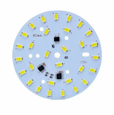
Larger photo of High Quality PCB for LED Lighting/Aluminum PCB
Related products about High Quality PCB for LED Lighting/Aluminum PCB
-
 Waste Tyre Plastic Recycling Machinery Machine Tire Crusher Production Line Rubber Crumb Grinding Machine Equipment Tire Shredder
-
 Stretch Plastic Blowing Pet Bottle Making Blow Molding Machine Bottles Stretch Automatic Pet Bottle Blowing Machine
-
 Waste Plastic Pet Bottle, Water Bottle Flake, PP/HDPE/LDPE PE Film Jumbo Woven Bags Plastic Crusher Machine, Plastic Crushing Washing Recycling Machine
-
 Type 2 Wall-Mounted Electric Car Charging Station 7kw /11 Kwelectric Vehicle Charging Station Home Wallbox AC EV Charger Single Phase or 3three Phase
-
 G-View G12W Wholesale Auto Car LED Headlight Bulb High Power H13 H11 9005 H7 H4 Car LED Headlights LED Car Lights
-
 New Design Porcelain Round Plates Dinner Set for Wedding and Banquet
-
 China 2023 New Design Super Soft 100% Polyester Microfiber Knitted Oversized Decoration Hoodie Blanket
-
 Handmade Art Creative Materials Thickened White Paper Cup DIY Disposable Handmade Colored Paper Cup


