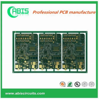
HDI PCB Boards Sucessful Cases Show-DefinitionHDI PCB is
defined as a printed circuit board with a higher wiring density per
unit area than a conventional PCB. They have much finer lines and
spaces, smaller vias and capture pads, and higher connection pad
density than employed in conventional PCB technology. HDI PCBs are
made through microvias, buried vias and sequential
lamination with insulation materials and conductor wiring for
higher density of routing.-ApplicationsHDI PCB is used to reduce
size and weight, as well as to enhance electrical performance of
the device. HDI PCB is the best alternative to high layer-count and
expensive standard laminate or sequentially laminated boards. HDI
incorporate blind and buried vias that help to
save PCB real estate by allowing features and lines to be
designed above or below them without making a connection. Many of
today's fine pitch BGA and flip-chip component footprints
do not allow for running traces between the BGA pads. Blind and
buried vias will only connect layers requiring connections in that
area.PCB CapabilitiesRigid PCB Manufacturing Capacity ABIS
experienced in making special materials for rigid PCB, such
as: CEM-1/CEM-3, PI, High Tg, Rogers, PTEF, Alu/Cu Base,
etc. Below is a brief overview
FYI. ItemSpeci.Layers1~20Board
Thickness0.1mm-8.0mmMaterialFR-4, CEM-1/CEM-3, PI, High Tg, Rogers,
PTEF, Alu/Cu Base, etcMax Panel Size600mm×1200mmMin Hole
Size0.1mmMin Line
Width/Space3mil(0.075mm)Board Outline Tolerance+_0.10mmInsulation Layer Thickness0.075mm--5.00mmOut Layer Copper Thickness18um--350umDrilling Hole (Mechanical)17um--175umFinish Hole (Mechanical)0.10mm--6.30mmDiameter Tolerance (Mechanical)0.05mmRegistration (Mechanical)0.075mmAspect Ratio16:1Solder Mask TypeLPISMT Mini. Solder Mask Width0.075mmMini. Solder Mask Clearance0.05mmPlug Hole Diameter0.25mm--0.60mmImpedance Control Tolerance+_10%Surface
finishENIG, OSP, HASL, Chem. Tin/Sn, Flash
GoldSoldermaskGreen/Yellow/Black/White/Red/BlueSilkscreenRed/Yellow/Black/WhiteCertificateUL,
ISO 9001, ISO14001, IATF16949 Special RequestBlind hole, Gold
finger, BGA, Carbon ink, peekable mask, VIP process, Edge plating,
Half holesMaterial SuppilersShengyi, ITEQ, Taiyo, etc.Common
PackageVacuum+Carton Lead TimePCB Lead
Time CategoryQ/T Lead timeStandard Lead TimeMass
Production Double Sided24hrs3-4 working days8-15 working
days 4 Layers48hrs3-5 working days10-15 working days 6
Layers72hrs3-6 working days10-15 working days 8 Layers96hrs3-7
working days14-18 working days 10 Layers120hrs3-8 working
days14-18 working days 12 Layers120hrs3-9 working days20-26
working days 14 Layers144hrs3-10 working days20-26 working
days 16-20 LayersDepends on the specific requirements 20+
LayersDepends on the specific requirementsOur AdvantagesHigh-end
euipment-high speed Pick and Place Machines that can process about
25,000 SMD components per hourHigh efficient supply ability 60K Sqm
monthly-Offers low volume and on-demand PCB production, also
large-scale productionProfessional engineering team-40 engineers
and their own tooling house, strong at OEM. Offers two easy
options: Custom and Standard-In-depth knowledge of IPC Class II and
III StandardsWe provide a comprehensive turn-key EMS service to
customers who want us to assemble the PCB into PCBA, including
prototypes, NPI project, small and medium volume. We are also able
to source all components for your PCB assembly project. Our
engineers and sourcing team have rich experience in supply chain
and EMS industry, with deep knowledges in SMT assembly allowing to
resolve all the production issues. Our service is cost-effective,
flexible, and reliable. We have satisfied customers across many
industries including medical, industrial, automotive and consumer
electronics. Quality ControlQuality
Control-Advanced equipment listAOI TestingChecks for solder
pasteChecks for components down to 0201Checks for missing
components, offset, incorrect parts, polarityX-Ray InspectionX-Ray
provides high-resolution inspection of:BGAs/Micro BGAs/Chip scale
packages /Bare boardsIn-Circuit TestingIn-Circuit Testing is
commonly used in conjunction with AOI minimizing functional defects
caused by component problems.Power-up TestAdvanced Function
TestFlash Device ProgrammingFunctional testing IOC incoming
inspectionSPI solder paste inspectionOnline AOI inspectionSMT first
article inspectionExternal assessmentX-RAY-welding inspectionBGA
device reworkQA inspectionAnti-static warehousing and
shipment-Persue 0% complaint on qualityAll department implements
according to ISO and the related dept has to provide 8D report if
any board scrapped to defective.All the outgoing boards have to be
100% electronic tested, impedance tested and soldering.Visual
inspected, we make the inspect microsection before shipment.Train
the mindset of employees and our enterprise culture, make they
happy with their work and our company, it's helpful for them to
produce good quality products.High quality raw material (Shengyi F
Quality Multilayer HDI Ccl Printed Circuit Board Custom HDI Printed Circuit Board Manufacturing China Supplier products, provide good price Multilayer HDI Ccl Printed Circuit Board Custom HDI Printed Circuit Board Manufacturing China Supplier from .
Related products about Multilayer HDI Ccl Printed Circuit Board Custom HDI Printed Circuit Board Manufacturing China Supplier
-
 Waste Tyre Plastic Recycling Machinery Machine Tire Crusher Production Line Rubber Crumb Grinding Machine Equipment Tire Shredder
-
 Stretch Plastic Blowing Pet Bottle Making Blow Molding Machine Bottles Stretch Automatic Pet Bottle Blowing Machine
-
 Waste Plastic Pet Bottle, Water Bottle Flake, PP/HDPE/LDPE PE Film Jumbo Woven Bags Plastic Crusher Machine, Plastic Crushing Washing Recycling Machine
-
 Type 2 Wall-Mounted Electric Car Charging Station 7kw /11 Kwelectric Vehicle Charging Station Home Wallbox AC EV Charger Single Phase or 3three Phase
-
 G-View G12W Wholesale Auto Car LED Headlight Bulb High Power H13 H11 9005 H7 H4 Car LED Headlights LED Car Lights
-
 New Design Porcelain Round Plates Dinner Set for Wedding and Banquet
-
 China 2023 New Design Super Soft 100% Polyester Microfiber Knitted Oversized Decoration Hoodie Blanket
-
 Handmade Art Creative Materials Thickened White Paper Cup DIY Disposable Handmade Colored Paper Cup


