Technical CapabilitiesItemsSpeci.RemarkMax panel size32" x
20.5"(800mm x 520mm) Max. Board size2000×610mm Min. board
Thickness2-layer 0.15mm 4-layer 0.4mm 6-layer
0.6mm 8-layer 1.5mm 10-layer 1.6~2.0mm Min. line
Width/Space0.1mm(4mil) Max. Copper thickness10OZ Min. S/M
Pitch0.1mm(4mil) Min. hole size0.2mm(8mil) Hole dia.
Tolerance (PTH)±0.05mm(2mil) Hole dia.
Tolerance,+0/-0.05mm(2mil) Hole position
deviation±0.05mm(2mil) Outline
tolerance±0.10mm(4mil) Twist & Bent0.75% Insulation
Resistance>10 12 Ω Normal Electric
strength>1.3kv/mm S/M abrasion>6H Thermal
stress288°C 10Sec Test Voltage50-300V Min. blind/buried
via0.15mm (6mil) Surface FinishedHASL, ENIG, ImAg, Imsn OSP,
Plating AG, Plating
gold MaterialsFR4,H-TG,Rogers,Ceramics,Aluminium, Copper
base Min trace width/ space (inner
layer)4mil/4mil(0.1mm/0.1mm) Min PAD (inner layer)5
mil(0.13mm)hole ring widthMin thickness(inner layer)4
mil(0.1mm)without copperInner copper thickness1~4 oz Outer
copper thickness0.5~6 oz Finished board thickness0.4-3.2
mm Board thickness tolerance control±0.10 mm±0.10 mm1~4
L±10%±10%6~8 L±10%±10%≥10 LInner layer treatmentbrown
oxidation Layer count Capability1-30 LAYER alignment
between ML±2mil Min drilling0.15 mm Min finished hole0.1
mm Hole precision±2 mil(±50 um) tolerance for
Slot±3 mil(±75 um) tolerance for PTH±3
mil(±75um) tolerance for NPTH±2mil(±50um) Max Aspect
Ratio for PTH08:01 Hole wall copper
thickness15-50um Alignment of outer layers4mil/4mil Min
trace width/space for outer layer4mil/4mil Tolerance of
Etching+/-10% Thickness of solder maskon
trace0.4-1.2mil(10-30um) at trace corner≥0.2mil(5um) On
base material≤+1.2mil Finished thicknessHardness of solder
mask6H Alignment of solder mask film±2mil(+/-50um) Min
width of solder mask bridge4mil(100um) Max hole with solder
plug0.5mm Surface finishHAL (Lead or Lead free), immersion
Gold, Immersion Nickel, Electric Gold finger,Electric Gold, OSP,
Immersion Silver. Max Nickel thickness for Gold
finger280u"(7um) Max gold thickness for Gold
finger30u"(0.75um) Nickel thickness in Immersion
Gold120u"/240u"(3um/6um) Gold thickness in Immersion
Gold2u"/6u"(0.05um/0.15um) Impedance control and its
tolerance50±10%,75±10%,100±10% 110±10% Trace Anti-stripped
strength≥61B/in(≥107g/mm) bow and twist0.75% 1.2m long
Aluminum Based PCB with LF HASL1. 1.2-1.5m extra Long Aluminium PCB
use in big studio and Gymnasium show lighting.2.PCB
Certificate:ISO UL REACH and RoHS3. Material:Aluminum4.Best price
with excellent after-service, 24 hours online serviceAll kinds of
high quality OEM PCB with fast delivery time and competitive
price is always our service. Welcome to contact us for
more details and talk further business.Inquiries are typically
answered within 24 hours .Wish you all the best and prosperous
business.the follow Picture is our Factory Drill Room
sight :) NOITEM MCPCB Technical capabilities1Layers1-3
layers2Max. Board size2000×610mm3Min. board Thickness1-layer
0.8mm2-layer 1.6mm3- layer 1.8mm 4Min. line
Width/Space0.2mm5Max. Copper thickness3 OZ6Min. S/M
Pitch0.15mm7Min. hole size0.6mm8Hole dia. Tolerance
(PTH)±0.05mm9Hole dia. Tolerance (NPTH)+0/-0.05mm10Hole position
deviation±0.05mm11Outline tolerance±0.10mm12Twist &
Bent0.75%13Insulation Resistance>10 12 ΩNormal14Electric
strength>1.3kv/mm15S/M abrasion>6H16Thermal stress288°C
20Sec17Test Voltage50-300V18Min. blind/buried via0.2 mm19Surface
FinishedHAL, ENIG, ImAg, Imsn OSP, Plating AG, Plating
gold20MaterialsFR4,H-TG,Rogers,Ceramics,Aluminium, Copper base/*
January 22, 2024 19:08:37 */!function(){function s(e,r){var
a,o={};try{e&&e.split(",").forEach(function(e,t){e&&(a=e.match(/(.*?):(.*)$/))&&1
Quality LED SMD PCB Board Reliable PCB Supplier for EMS/OEM Customers & Trading Companies products, provide good price LED SMD PCB Board Reliable PCB Supplier for EMS/OEM Customers & Trading Companies from Shenzhen Okey Circuit Co., Ltd..
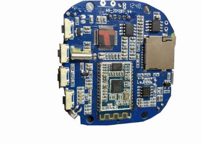
Larger photo of LED SMD PCB Board Reliable PCB Supplier for EMS/OEM Customers & Trading Companies
Related products about LED SMD PCB Board Reliable PCB Supplier for EMS/OEM Customers & Trading Companies
-
 Waste Tyre Plastic Recycling Machinery Machine Tire Crusher Production Line Rubber Crumb Grinding Machine Equipment Tire Shredder
-
 Stretch Plastic Blowing Pet Bottle Making Blow Molding Machine Bottles Stretch Automatic Pet Bottle Blowing Machine
-
 Waste Plastic Pet Bottle, Water Bottle Flake, PP/HDPE/LDPE PE Film Jumbo Woven Bags Plastic Crusher Machine, Plastic Crushing Washing Recycling Machine
-
 Type 2 Wall-Mounted Electric Car Charging Station 7kw /11 Kwelectric Vehicle Charging Station Home Wallbox AC EV Charger Single Phase or 3three Phase
-
 G-View G12W Wholesale Auto Car LED Headlight Bulb High Power H13 H11 9005 H7 H4 Car LED Headlights LED Car Lights
-
 New Design Porcelain Round Plates Dinner Set for Wedding and Banquet
-
 China 2023 New Design Super Soft 100% Polyester Microfiber Knitted Oversized Decoration Hoodie Blanket
-
 Handmade Art Creative Materials Thickened White Paper Cup DIY Disposable Handmade Colored Paper Cup


