Product Features MTP/MP0 optical connector Single +3.3V power
supply Hot-pluggable QSFP28 MSA form factor Up to 100m OM4 MMF
Distance 4x28G Electrical Serial Interface (CEI-28G-VSR) AC
coupling of CML signals Low power dissipation(Max:3.5W) Built in
digital diagnostic function Operating case temperature range:0ºC to
70ºC Compliant with 100GBASE-SR4 I2C Communication Interface
Applications 100GBASE-SR4 Infiniband QDR/DDR/SDR 100G Datacom
connections Standards Compliant with IEEE 802.3ba Compliant
with QSFP28 MSA hardware specifications Compliant with RoHS
Functional Description The 100G QSFP28 SR4 optical transceiver
integrates the transmit and receive path onto one module. It
converts parallel electrical input signals into parallel optical
signals, by a driven Vertical Cavity Surface Emitting Laser (VCSEL)
array. The transmitter module accepts electrical input signals
compatible with Common Mode Logic (CML) levels. All input data
signals are differential and internally terminated. The receiver
module converts parallel optical input signals via a photo detector
array into parallel electrical output signals. The reCML) levels.
All data signals are differential and support a data rates up to
27.9525Gb/s per channel.ceiver module outputs electrical signals
are also voltage compatible with Common Mode LogicOn This module
features a hot-pluggable electrical interface, low power
consumption, and 2-wire serial interface.Absolute Maximum
Ratings ParameterSymbolMin.Max.UnitNoteSupply
VoltageVcc-0.53.6V Storage TemperatureTS-4085°C Relative
HumidityRH085% Rx Damage Threshold,per
LanePRdmg5.5 dBm Note: Stress in excess of the
maximum absolute ratings can cause permanent damage to the
transceiver.Recommended Operating
ConditionsParameterSymbolMinTypMaxUnitsNoteOperating Case
TemperatureTC0-+70°C Power Supply
VoltageVCC3.143.33.47V Data
rate 103.125112Gb/s Link Distance
(OM3) 70m Link Distance
(OM4) 100m Electrical Characteristics
(Top=0~70ºC, Vcc=3.14~3.47V)(Tested under recommended operating
conditions,unless otherwise noted)
ParameterSymbolMinTypMaxUnitNotesTransmitterSignaling rate per
laneDRPL25.78125 ± 100 ppmGb/s Differential pk-pk input
voltage toleranceVin,dpp 900mV Single-ended voltage
toleranceVin,pp-0.35 +3.3V Module stress input
test Per IEEE 802.3bm ReceiverSignaling rate per
laneDRPL25.78125 ± 100 ppmGb/s Differential data output
swingVout,pp400 800mV Eye
widthEw0.57 UI Vertical eye
closureVEC5.5 dB Differential termination
mismatchTm 10% Transition time, 20% to
80%Tr,Tf12 ps Optical Characteristics (Top=0~70ºC,
Vcc=3.14~3.47V)(Tested under recommended operating
conditions,unless otherwise noted)
ParameterSymbolUnitMinTypMaxNotesTransmitterSignaling rate, each
laneDRplGb/s25.78125 ±100 ppm1Center
Wavelengtheλnm840850860 RMS Spectral
Width nm 0.6 Average launch power, each
lanePavgdBm-8.4 2.4 Optical modulation amplitude, each
lane (OMA)OMAdBm-6.4 3 Extinction
ratioERdB2 Average Launch Power of OFF
Transmitter, per LaneRINdBm -30 Encircled
FluxFLXdBm>86% at 19 um
Quality RoHS Compliant 100GB/S Qsfp28 Sr4 100m Optical SFP Transceiver products, provide good price RoHS Compliant 100GB/S Qsfp28 Sr4 100m Optical SFP Transceiver from .
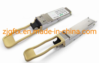
Larger photo of RoHS Compliant 100GB/S Qsfp28 Sr4 100m Optical SFP Transceiver
Related products about RoHS Compliant 100GB/S Qsfp28 Sr4 100m Optical SFP Transceiver
-
 Waste Tyre Plastic Recycling Machinery Machine Tire Crusher Production Line Rubber Crumb Grinding Machine Equipment Tire Shredder
-
 Stretch Plastic Blowing Pet Bottle Making Blow Molding Machine Bottles Stretch Automatic Pet Bottle Blowing Machine
-
 Waste Plastic Pet Bottle, Water Bottle Flake, PP/HDPE/LDPE PE Film Jumbo Woven Bags Plastic Crusher Machine, Plastic Crushing Washing Recycling Machine
-
 Type 2 Wall-Mounted Electric Car Charging Station 7kw /11 Kwelectric Vehicle Charging Station Home Wallbox AC EV Charger Single Phase or 3three Phase
-
 G-View G12W Wholesale Auto Car LED Headlight Bulb High Power H13 H11 9005 H7 H4 Car LED Headlights LED Car Lights
-
 New Design Porcelain Round Plates Dinner Set for Wedding and Banquet
-
 China 2023 New Design Super Soft 100% Polyester Microfiber Knitted Oversized Decoration Hoodie Blanket
-
 Handmade Art Creative Materials Thickened White Paper Cup DIY Disposable Handmade Colored Paper Cup


